


Tech
Understanding NR-V2X: Next Generation V2X Communication
Are you ready for the next big thing in vehicle communication technology? Well, get ready to buckle up because NR-V2X is here and it’s taking the automotive industry by storm! As the latest generation of V2X (vehicle-to-everything) communication, NR-V2X has revolutionized how vehicles interact with each other and their environment. In this blog post, we’ll take a deep dive into understanding what exactly NR-V2X is all about and why it’s such a game-changer for connected cars. So sit tight and let’s explore this exciting new technology together!
What is NR-V2X?
NR-V2X is a form of Vehicle-to-Everything (V2X) communication that uses the 5G New Radio (NR) standard to enable wireless communication between vehicles, infrastructure, and other devices. It is a newer version of the existing V2X technology, which has been widely used for several years, but with improved capabilities and features.
The History of NR-V2X
The development of NR-V2X began in the early 2010s, as researchers and industry leaders recognized the need for a more advanced and reliable V2X communication standard. In 2017, the 3rd Generation Partnership Project (3GPP) – an international organization responsible for developing global telecommunications standards – announced that it would incorporate NR-V2X into its 5G specifications. This move was seen as a significant step forward for the technology, as it would enable NR-V2X to leverage the benefits of 5G networks, such as faster data speeds, lower latency, and improved reliability.
Why was NR-V2X developed?
NR-V2X was developed to improve the safety and efficiency of road transportation by enabling real-time communication between vehicles, infrastructure, and other devices. By providing vehicles with advanced warning of potential hazards, such as accidents or traffic congestion, NR-V2X can help drivers to make safer and more informed decisions. It can also enable more efficient traffic flow and reduce congestion, by allowing vehicles to communicate with traffic lights and other infrastructure in real-time.
Features of NR-V2X
NR-V2X includes several advanced features that set it apart from previous V2X standards. One key feature is the ability to operate in both the 5.9 GHz Dedicated Short-Range Communications (DSRC) band and the 5G New Radio (NR) band. This flexibility allows NR-V2X to work with a wider range of devices and networks, improving its interoperability and compatibility with existing infrastructure.
NR-V2X also includes advanced security and privacy features, such as encryption and digital signatures, to protect against unauthorized access and ensure the privacy of communication between devices.
Additionally, NR-V2X supports advanced positioning capabilities, such as Global Navigation Satellite System (GNSS) and 3D mapping, which can provide highly accurate location data for vehicles and other devices. This data can be used for a range of applications, such as collision avoidance and traffic management.
Applications of NR-V2X
NR-V2X has a wide range of potential applications in the transportation sector, from improving road safety to enabling autonomous driving. One key application is collision avoidance, which can use NR-V2X to alert drivers of potential hazards, such as other vehicles or pedestrians, in real-time. This feature can be particularly useful in complex driving environments, such as urban areas or highways.
NR-V2X can also be used to enable more efficient traffic flow, by providing real-time data on road conditions and enabling vehicles to communicate with traffic lights and other infrastructure. This can help to reduce congestion and improve overall traffic flow.
Additionally, NR-V2X has potential applications in autonomous driving, where it can be used to provide highly accurate location data and enable communication between autonomous vehicles and other devices. This can help to improve the safety and efficiency of autonomous driving systems, enabling them to make more informed decisions based on real-time data.
NR-V2X is a new and advanced form of V2X communication that leverages the benefits of the 5G New Radio standard to enable real-time communication between vehicles, infrastructure, and other devices. With its advanced features and capabilities, NR-V2X has the potential to revolutionize the transportation sector, improving road safety, reducing congestion, and enabling more efficient and autonomous driving systems. As the technology continues to evolve

Automotive
The Rise of System-in-Package (SiP): How Advanced IC Packaging Is Redefining Electronics Miniaturization
Summary: System-in-Package (SiP) technology is one of the fastest-growing segments in semiconductor packaging, driven by demand for compact, high-performance devices across healthcare, defense, aerospace, and consumer electronics.
This article covers: what SiP is and why it matters; key market trends and drivers; the technical challenges facing engineers; the landscape of existing solutions; and how an all-in-one manufacturing approach delivers a competitive edge in SiP design and production.
As electronics continue to shrink while demands for performance grow, the industry faces a pivotal inflection point. For engineers and product teams researching IC packaging companies capable of delivering complete SiP solutions, understanding the full technology landscape has never been more important.
What Is System-in-Package and Why Does It Matter?
System-in-Package (SiP) is a technology approach that integrates multiple functional components – processors, memory, sensors, RF modules, and passive components – into a single compact package. Unlike a System-on-Chip (SoC), which integrates all functions onto a single die, SiP combines multiple dies and components, often using different process nodes, into one unified module.
This heterogeneous integration approach offers a powerful alternative to traditional multi-chip designs, addressing the core engineering tradeoffs of size, performance, power consumption, and cost. As consumer electronics, wearables, industrial IoT devices, and defense electronics demand ever-smaller form factors without sacrificing functionality, SiP has emerged as a foundational technology for the next generation of electronic systems.
Market Trends Driving SiP Adoption
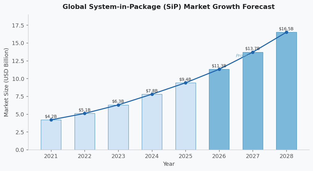
The global SiP market is on a steep growth trajectory. According to industry research, the market was valued at approximately $8 billion in 2024 and is forecast to approach $17 billion by 2028, growing at a compound annual rate exceeding 15%. Several macro trends are powering this expansion:
- IoT and Wearable Devices: The explosion of connected devices demands ultra-compact, low-power modules. SiP allows designers to integrate sensing, processing, and connectivity functions into a package small enough for a smartwatch or medical implant.
- 5G and Advanced Communications: Millimeter-wave 5G systems require highly integrated RF front-end modules. SiP enables the co-packaging of RF components with antenna structures, dramatically reducing signal loss and board real estate.
- Defense and Aerospace Miniaturization: Modern defense electronics – from drone guidance systems to soldier-worn electronics – require extreme miniaturization alongside ultra-high reliability under harsh environmental conditions.
- Medical Device Innovation: Implantable devices, hearing aids, and continuous health monitors are pushing miniaturization to new extremes, where SiP technology enables life-critical functionality in sub-centimeter packages.
- Automotive Electronics: Advanced driver-assistance systems (ADAS) and autonomous vehicle platforms require high-density, thermally reliable SiP modules capable of operating across extreme temperature ranges.
The Technical Challenges of SiP Design and Manufacturing
While SiP offers compelling advantages, its design and manufacturing complexity is substantial. Engineers face a constellation of technical challenges that require deep, cross-domain expertise:
- Thermal Management: Integrating multiple high-power components into a small package concentrates heat significantly. Ensuring reliable thermal dissipation without increasing package height or weight requires sophisticated substrate engineering, embedded coin technology, and careful die placement.
- Signal Integrity and Electromagnetic Interference (EMI): Heterogeneous integration creates complex signal routing challenges. Fine-pitch interconnects between dies must maintain controlled impedance while minimizing crosstalk and EMI – particularly critical in RF and high-speed digital applications.
- CTE Mismatch: Different materials – silicon dies, organic substrates, and passive components – expand and contract at different rates under thermal cycling. Managing coefficient of thermal expansion (CTE) mismatches is essential for long-term reliability, especially in aerospace and defense applications where temperature extremes are the norm.
- Supply Chain Complexity: Traditional SiP development requires coordinating multiple specialized vendors for substrate fabrication, die sourcing, assembly, and testing. Each handoff introduces risk, delay, and potential quality variation.
- Design for Testability: Testing a fully assembled SiP module is fundamentally more difficult than testing individual components. Embedded dies and multi-layer substrates limit physical access, requiring sophisticated In-Circuit Testing (ICT) and system-level test strategies.
The Landscape of SiP Solutions Today
The market has responded to SiP complexity in several ways. Large Outsourced Semiconductor Assembly and Test (OSAT) companies offer high-volume SiP assembly, but their minimum order quantities and standardized processes are often mismatched with the prototype-to-mid-volume needs of defense, aerospace, and medical device companies. Dedicated substrate foundries provide advanced substrate technology but require separate assembly and test partners, fragmenting the supply chain.
The result is that many engineering teams face a frustrating choice: accept the limitations of standardized, high-volume OSAT services, or manage a complex multi-vendor supply chain that introduces quality risk and schedule uncertainty. A third path – working with an integrated, all-in-one solutions provider – is increasingly recognized as the most effective approach for complex, high-reliability SiP programs.
For a deeper understanding of the academic and technical foundations of SiP development, the IEEE Xplore library provides extensive peer-reviewed research on heterogeneous integration, organic substrates, and advanced packaging reliability testing.
How an All-in-One Approach Addresses SiP Complexity
PCB Technologies, with its specialized iNPACK division, has built an integrated capability that directly addresses the core challenges of SiP development. As described on their website, the company is an “All-in-One Solutions Provider of Miniaturization & Advanced IC Packaging Solutions,” operating with a single-roof approach that spans design, substrate fabrication, package assembly, and testing.
Their iNPACK division offers advanced System-in-Package solutions as multi-component, multifunction products. Key capabilities include size reduction, high thermal conductivity, ultra-thin substrates with fine lines and spacing, controlled CTE, 3D design, shielding options, sealing solutions, fine-pitch flip-chip and copper pillar technology, double-side assembly, development and production testing, and full turnkey solutions.
A core differentiator of iNPACK is its organic substrate technology, supporting 25-micron lines and 25-micron spacing – precision that enables the fine-pitch signal routing critical to advanced SiP applications. Their on-site, certified cleanroom manufacturing facility ensures that sensitive components remain free from contamination throughout the assembly process.
Critically, PCB Technologies’ approach eliminates the multi-vendor fragmentation that plagues many SiP programs. Their R&D center is located within the same complex as their manufacturing facilities, enabling seamless transitions from design iteration to prototype production without the handoff delays and communication gaps inherent in fragmented supply chains.
For engineers exploring panel level packaging as an alternative to wafer-level processes, iNPACK’s panel-level approach uses rectangular panels similar to organic substrate manufacturing – designed for efficient production, lower cost per unit, and the flexibility to incorporate Multi-Chip Module (MCM) and SiP assembly on the same production infrastructure.
SiP in Practice: Applications Across High-Demand Industries
The industries best positioned to leverage SiP technology share a common need: maximum functionality in minimum space, with uncompromising reliability. PCB Technologies serves customers across medical, defense, aerospace, communications, and semiconductor sectors – all of which are increasingly turning to SiP as a strategic platform.
- Defense Electronics: Miniaturized radar modules, electronic warfare systems, and soldier-worn communications devices require SiP solutions that maintain performance under shock, vibration, and extreme temperatures. High-reliability SiP with embedded thermal management meets these requirements.
- Medical Devices: From cochlear implants to continuous glucose monitors, medical SiP modules must combine RF, sensing, and processing in biocompatible packages that meet ISO 13485 quality standards – a certification held by PCB Technologies.
- IoT and Industrial Systems: Industrial IoT nodes that operate in harsh environments require rugged SiP modules with wide operating temperature ranges, integrated sensing, and low-power wireless connectivity.
Conclusion: SiP Is No Longer Optional — It Is a Strategic Imperative
System-in-Package technology has moved from a niche solution for space-constrained applications to a mainstream platform technology across multiple high-growth industries. For product teams facing the dual pressure of miniaturization and performance, SiP is increasingly the answer – but only when implemented with the right combination of substrate expertise, assembly precision, and integrated design-to-test capability.
The companies that will lead in the next wave of electronics miniaturization will be those that choose manufacturing partners capable of delivering SiP solutions as an end-to-end, accountable service – from substrate design through final system testing, all under one roof.
Summary: IC interconnect technology – how a semiconductor die connects electrically to its substrate or package – is one of the most consequential decisions in modern electronics design.
This article examines: the technical fundamentals of wire bonding and flip chip packaging; the market trends reshaping interconnect technology choices; the engineering tradeoffs that determine which approach is optimal for a given application; the landscape of available solutions; and how an integrated packaging capability enables engineers to access both technologies – and choose freely between them – within a single supply chain.
For engineers evaluating interconnect strategies for their next design, understanding the full depth of wire bonding options and their flip chip alternatives is essential. The choice directly affects device performance, package size, signal integrity, manufacturing cost, and qualification timeline.
The Fundamentals: What Wire Bonding and Flip Chip Actually Are
At its core, the IC interconnect challenge is straightforward: a semiconductor die contains hundreds or thousands of tiny electrical contact pads. Those pads must be connected to the package substrate – which then connects to the PCB – with minimal resistance, inductance, and crosstalk, while maintaining mechanical integrity through thermal cycling, vibration, and shock.
Wire Bonding is the oldest and most widely used interconnect technique. Thin wires – typically gold, copper, or aluminum – are bonded from the die bond pads to the package substrate using thermal compression, ultrasonic energy, or a combination of both (thermosonic bonding). The resulting wire loops are visible under a microscope as delicate arcs spanning from die to substrate.
Flip Chip packaging inverts this approach. Instead of bonding wires from the top surface of the die, the die is flipped face-down, with solder bumps or copper pillars on the active surface connecting directly to matching pads on the substrate. The entire connection is made through these bumps in a single reflow step, with no wire loops.
Market Trends: The Steady Rise of Flip Chip
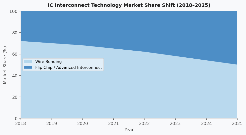
The global IC packaging market is undergoing a structural shift away from wire bonding as the dominant interconnect approach, driven by the performance demands of advanced applications. Industry research indicates that flip chip packaging now accounts for roughly half of the total IC interconnect market by value, with penetration continuing to grow in high-performance segments.
Several converging trends are driving this shift:
- High-Speed Digital Performance: Modern processors, memory controllers, and network chips operate at speeds where wire inductance – an inherent characteristic of wire bond loops – causes signal integrity problems. Flip chip’s shorter, lower-inductance interconnects are essential for chips operating above a few gigahertz.
- Fine-Pitch I/O Requirements: As die complexity increases, the number of I/O connections grows and their pitch shrinks. Advanced chips now require hundreds to thousands of I/O connections at pitches that wire bonding cannot reliably achieve, but flip chip copper pillars can support.
- Thermal Performance: Flip chip’s inverted die placement exposes the back side of the silicon directly upward, enabling direct attachment of a heatsink to the die – dramatically improving thermal dissipation compared to wire bonded packages where the die back faces the substrate.
- Package Height Reduction: Wire bond loops require vertical clearance above the die. Flip chip eliminates this requirement, enabling ultra-thin packages critical for wearables, implantable medical devices, and ultra-thin consumer electronics.
Where Wire Bonding Remains the Optimal Choice
Despite the growth of flip chip, wire bonding is far from obsolete – and for many applications, it remains the technically and economically optimal choice.
- Cost-Sensitive, Standard I/O Applications: Wire bonding equipment and processes are mature, widely available, and highly cost-effective for chips with moderate I/O counts and standard pitch. For commodity sensors, microcontrollers, and discrete semiconductors, wire bonding delivers excellent performance at minimal cost.
- Mixed-Die Assemblies: In multi-chip module (MCM) designs and System-in-Package (SiP) assemblies, wire bonding enables flexible interconnection between dies of different sizes and heights – including die-to-die connections within the same package that would be impractical with bump-based approaches.
- Known-Good Die (KGD) Management: Wire bonding can be performed after functional testing of individual dies, reducing the risk of assembling expensive SiP modules with defective components.
- Rework Capability: Wire bonds can be selectively reworked – broken bonds can be re-bonded – providing a repair option that flip chip assemblies generally do not offer, which is valuable in low-volume, high-value applications.
Flip Chip vs. Wire Bond: The Engineering Decision Framework
The choice between flip chip vs wire bond is not a binary decision with a universal right answer. It is a multi-dimensional optimization across performance, cost, form factor, reliability, and supply chain complexity. The key decision drivers include:
- Operating Frequency: For applications below approximately 1 GHz, wire bonding is typically sufficient. For RF, mmWave, and high-speed digital applications above a few GHz, flip chip’s lower parasitics become essential.
- I/O Count and Pitch: For designs with more than a few hundred I/O at fine pitch, flip chip or copper pillar technology is generally required. Wire bonding becomes physically impractical at very high I/O densities.
- Package Thickness: For applications where vertical space is at a premium, flip chip eliminates the wire loop height overhead – typically 200–400 microns – enabling thinner packages.
- Thermal Requirements: High-power dies benefit significantly from the superior thermal path provided by direct heatsink attachment enabled by flip chip orientation.
- Volume and Cost Sensitivity: At low-to-medium volumes, wire bonding is typically more cost-effective. At high volumes, the economics become more application-specific and are influenced heavily by substrate cost, yield, and test strategy.
The Integration Advantage: Access to Both Technologies in One Supply Chain
One of the most underappreciated challenges in advanced IC packaging is the supply chain fragmentation that results when different interconnect technologies require different vendors. Many organizations source wire bonding from one assembly house, flip chip from another, and organic substrates from a third – creating a coordination burden that adds time, cost, and quality risk to every program.
PCB Technologies, through its iNPACK division, offers a fundamentally different model. As described in their materials, the iNPACK division provides complete package PCB assembly solutions including SiP design and manufacturing, surface mount technology, chip on board (COB) wire bonding, microfabrication, and substrate design and manufacturing – all under one roof.
Their substrate technology supports 25-micron lines and 25-micron spacing, enabling the fine-pitch routing required for both advanced wire bond fan-out designs and flip chip copper pillar interconnects. Their cleanroom manufacturing facility, certified to ISO 9001, ISO 14001, ISO 13485, and AS 9100, ensures the contamination control and process discipline required for reliable advanced interconnects.
For engineers seeking academic grounding in IC interconnect technologies, IEEE Xplore provides extensive peer-reviewed literature on wire bonding reliability, flip chip process development, and advanced packaging interconnect performance – an essential reference for teams evaluating interconnect technology choices.
The Path Forward: Heterogeneous Integration
The most sophisticated packaging programs today do not choose between wire bonding and flip chip – they use both, strategically, within the same SiP module. A high-power processor might use copper pillar flip chip interconnects for maximum performance, while peripheral functions such as a power management IC, a sensor die, or an RF module are wire bonded to the same substrate.
This heterogeneous integration approach requires the substrate to accommodate both interconnect types simultaneously, with the DfM expertise to ensure that both are manufacturable, testable, and reliable at production scale. It is a capability that demands deep, integrated expertise across substrate design, interconnect technology, assembly process, and test engineering.
Conclusion: The Right Interconnect for the Right Application
Wire bonding and flip chip packaging represent complementary – not competing – technologies in the modern IC packaging toolkit. The engineering challenge is not to choose one universally, but to understand each application’s specific requirements deeply enough to select the right approach, and to partner with a manufacturing organization capable of executing either strategy with equal precision and accountability.
As miniaturization continues to advance and new application categories – implantable medical devices, next-generation defense electronics, advanced automotive systems – push the boundaries of what is possible, the ability to access both interconnect technologies through a single, integrated supply chain will increasingly determine which organizations can deliver on their design intent.
Business Solutions
Optical Delay Lines: The Precision Solution Reshaping Radar and Altimeter Testing
Summary: Radar and altimeter systems must be rigorously tested and calibrated before deploymen-but transmitting live RF energy to simulate target returns is impractical, hazardous, and often impossible in a laboratory or depot environment. This article explains how optical delay lines (ODLs) solve this fundamental challenge, how they work, why fiber-based delay lines outperform electronic alternatives, and how RFOptic’s specialized ODL solutions support radar and altimeter testing programs across defense and aviation markets.
Radar and altimeter testing is one of the most technically demanding areas in defense electronics validation. Systems must be verified to perform accurately across a range of simulated target distances, velocities, and environments-yet doing so by physically placing reflecting targets at the required distances is seldom feasible. The solution lies in optical delay lines, a technology that uses the fixed propagation speed of light in optical fiber to introduce precisely controlled time delays into an RF signal, simulating the time-of-flight of a radar return at a specified range.
The Testing Problem: Why You Cannot Simply Transmit to a Real Target
A radar system determines the range of a target by measuring the round-trip time of a transmitted pulse. An altimeter determines altitude by measuring the time for the transmitted signal to reflect off the ground and return. In both cases, the fundamental measurement is time-of-flight -and testing this measurement requires introducing a known, accurate delay between the transmitted signal and the simulated return.
In field testing, this can be done by physically placing a reference reflector at a known distance. But field testing is expensive, weather-dependent, logistically complex, and often impossible for airborne altimeters (which would require flight testing to validate each range point) or for classified radar systems that cannot be operated in environments where frequency emissions are monitored or regulated. Depot-level maintenance and factory acceptance testing require a bench solution.
Electronic delay lines-switched networks of lumped inductors and capacitors, or surface acoustic wave (SAW) devices-have historically been used for this purpose. But they carry significant limitations: limited frequency range, high insertion loss, temperature-dependent performance, and the inability to cover the multi-microsecond delays needed to simulate distant targets without cascading multiple stages and accumulating noise and distortion.
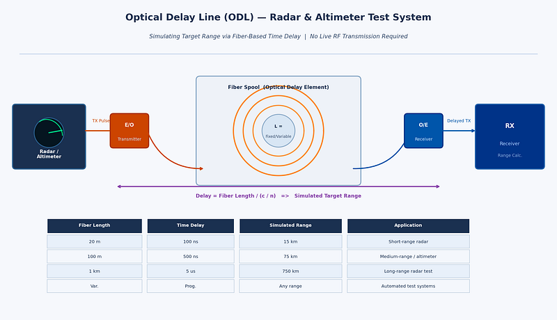
How an Optical Delay Line Works
An optical delay line converts the RF signal to be delayed into an optical signal using an electro-optic modulator or laser diode, routes that optical signal through a calibrated length of single-mode optical fiber, then reconverts it back to an RF signal at the output using a photodetector. Since light travels through fiber at approximately 2×1⁰⁸ meters per second (about two-thirds of the speed of light in vacuum), a specific fiber length produces a very precise and stable delay.
For example, approximately 100 meters of fiber produces a delay of around 500 nanoseconds-equivalent to a radar range of approximately 75 kilometers in a monostatic radar configuration. Variable delay lengths can be achieved through switched fiber spools, allowing test equipment to simulate targets at multiple programmable ranges without moving any physical hardware.
The key performance advantages of fiber-based delay lines compared to electronic alternatives are:
• Extremely low loss: optical fiber introduces negligible signal loss per unit length compared to coaxial cable or electronic delay elements at microwave frequencies.
• Frequency independence: the delay is determined purely by the fiber length, not the frequency of the signal. The same ODL works equally well at 1 GHz and at 40 GHz, making it suitable for multi-band radar and wideband altimeter testing.
• Excellent phase stability: fiber delay is not affected by electromagnetic interference and shows very low thermal drift compared to electronic delay networks.
• Scalability: very long delays (microseconds to tens of microseconds) equivalent to hundreds or thousands of kilometers of range-are achievable simply by using more fiber, without cascading lossy electronic stages.
• Electrical isolation: optical fiber passes no DC current and provides complete galvanic isolation between the input and output RF ports, eliminating common-ground interference paths in complex test setups.
Variable and Programmable Optical Delay Lines
The most operationally useful ODL systems offer variable or programmable delay-the ability to switch between multiple discrete delay values to simulate different target ranges. This is achieved through optical switching networks that connect the RF signal to different fiber spools of different lengths, or through continuous variable delay mechanisms using motorized fiber stretchers or optical path length adjustment.
Programmable delay lines are essential for acceptance testing of radar systems that must perform across the full specified range envelope. Rather than resetting physical hardware for each range point, the test engineer selects the desired delay from the ODL’s control interface, and the system switches to the appropriate fiber path within milliseconds. For automated production test environments, this enables rapid, software-controlled multi-point range calibration.
According to the IEEE Transactions on Microwave Theory and Techniques, optical delay line technology has advanced considerably with the integration of programmable switching and temperature compensation, making modern ODL systems suitable for demanding calibration environments where measurement uncertainty must be minimized.
Altimeter Testing: A Specialized Requirement
Radio altimeters-used in commercial aviation, military aircraft, and UAVs to measure height above terrain-are safety-critical systems with stringent testing requirements. Regulatory bodies including the FAA and EASA require verification of altimeter accuracy across the full operating altitude range, typically from near-zero to several thousand feet. Testing each altitude point requires introducing the corresponding time delay between the transmitted altimeter signal and the simulated ground return.
Modern radar altimeters typically operate in the 4.2–4.4 GHz frequency band, though next-generation systems and those for unmanned platforms span wider ranges. Key testing parameters include:
• Absolute accuracy: the altimeter must measure altitude to within a defined tolerance across the full range.
• Response time: the altimeter must update its reading within a specified latency when altitude changes rapidly-important for terrain-following and automatic landing systems.
• Interference immunity: with 5G networks now deployed in the 3.7–4.2 GHz C-band in many countries, regulatory concerns about altimeter interference have made test coverage of adjacent-band interference scenarios a new requirement.
An optical delay line test system for altimeter applications must cover the altimeter’s full altitude range (typically equivalent to delays from a few to several hundred nanoseconds), handle the altimeter’s specific frequency band, and provide calibrated, repeatable delay values. For aircraft integration testing, the system must also operate reliably in the electromagnetic environment of an avionics test bench.
RFOptic’s Optical Delay Line Solutions
RFOptic offers customized low and high frequency optical delay line solutions for testing and calibrating radar and altimeter systems. The company’s ODL product line is described as one of its core competencies, offering both standard and application-specific configurations.
RFOptic provides both fixed and programmable delay configurations, with the following key characteristics as described on their platform:
• Coverage from low frequency through high-frequency microwave and mmWave bands, supporting both current-generation radar and altimeter systems and next-generation wideband applications.
• Customized ODL systems developed to customer specifications, including integration with specific test equipment interfaces and control software.
• Online request-for-quote tool for customized ODL and altimeter ODL systems, supporting design consultation from the earliest project stage.
• Subsystem integration: RFOptic’s ODLs can be integrated into complete radar and altimeter test subsystems, combining the delay function with signal conditioning, switching, and management interfaces.
RFOptic’s value proposition emphasizes that in the pre-sales stage, the company builds solutions tailored to customer needs, including simulations that predict link behavior-particularly important for ODL systems where target delay accuracy and dynamic range must be verified analytically before hardware is built.
Emerging Applications: UAV Altimeters and Radar Testing
The rapid growth of unmanned aerial systems (UAS/UAV) has created a new generation of altimeter testing requirements. Drone altimeters are smaller, lighter, and often operate in different frequency bands than traditional aviation altimeters. They must be validated for low-altitude terrain-following, precision landing approaches, and operation in spectrum-contested environments. The same fundamental principle applies: fiber-based optical delay lines provide the most accurate and flexible platform for simulating the required altitude ranges in a laboratory setting.
For those evaluating radar testing solutions, the combination of programmable delay ranges, wide frequency coverage, and low noise floor that optical delay lines provide makes them the reference tool of choice across military radar, commercial aviation, and UAV development programs.
Conclusion
Optical delay lines represent a technically elegant solution to one of the oldest problems in radar and altimeter development: how to test time-of-flight accuracy without deploying hardware into the field. By leveraging the fixed and stable propagation speed of light in optical fiber, ODL systems deliver highly accurate, repeatable, and frequency-independent delay values that electronic alternatives cannot match at microwave and mmWave frequencies.
For radar system developers, avionics test labs, and depot maintenance facilities, investing in optical delay line test equipment-particularly programmable systems capable of simulating multiple range points-is a practical step that reduces test time, improves calibration accuracy, and future-proofs the test infrastructure for next-generation wideband radar and altimeter systems.
The Rise of System-in-Package (SiP): How Advanced IC Packaging Is Redefining Electronics Miniaturization
Wire Bonding vs. Flip Chip: Navigating the Evolving World of IC Interconnect Technology
Optical Delay Lines: The Precision Solution Reshaping Radar and Altimeter Testing

-
Business Solutions2 years ago
Understanding A2P Messaging and the Bulk SMS Business Landscape
-

 Business Solutions2 years ago
The Power of Smarts SMS and Single Platform Chat Messaging
-
 Automotive3 years ago
DSRC vs. CV2X: A Comprehensive Comparison of V2X Communication Technologies
-

 Business Solutions2 years ago
Exploring OTP Smart Features in Smart Messaging Services
-

 Business Solutions2 years ago
Live Video Broadcasting with Bonded Transmission Technology
-

 Business Solutions10 months ago
The Future of Healthcare SMS and RCS Messaging
-

 Business Solutions2 years ago
2-Way Texting Solutions from Company Message Services
-

 Business Solutions2 years ago
Communication with Analog to Fiber Converters & RF Link Budgets